Navitas Semiconductor, Industry-Leader in Gallium Nitride Power ICs, Announces Acquisition of GeneSiC Semiconductor, Silicon Carbide Pioneer


El Segundo, CA., August 15th, 2022 — Navitas Semiconductor (Nasdaq: NVTS), the industry leader in gallium nitride (GaN) power ICs, today announced the acquisition of GeneSiC Semiconductor, a silicon carbide (SiC) pioneer with deep expertise in SiC power device design and process. The transaction is immediately accretive to Navitas as GeneSiC is highly profitable, with more than 25% EBITDA margins.  Calendar 2022 revenues are expected to be approximately $25 million with demonstrated annual growth rates of over 60%. The combined company creates a comprehensive, industry-leading technology portfolio in next-generation power semiconductors – both GaN and SiC – with an aggregate market opportunity estimated at over $20 billion per year by 2026.

“GeneSiC is an ideal partner for Navitas with their focus and success in developing industry-leading SiC technology,” said Gene Sheridan, Navitas CEO and co-founder. “Navitas has significant investments in global sales, operations and technical support teams, along with system design centers in EV and data centers. These capabilities are a perfect complement to GeneSiC and will further accelerate their growth in both synergistic and new customers and markets. Today, we have taken a major step in our company’s mission to ‘Electrify Our World™’ and drive our planet’s transition from fossil fuels to clean,      efficient, electrical energy.”

“GeneSiC’s patent-protected, advanced technology and innovative, experienced team are critical factors in the growth of our company. Our SiC MOSFETs offer the industry’s highest performance, reliability, and ruggedness – parameters critical towards widespread adoption of electric vehicles and associated infrastructure,” said GeneSiC President Dr. Ranbir Singh. “With almost 20 years of leading-edge R&D, proven platforms, over 500 diverse customers, and growing revenue and profitability, we can leverage Navitas’ mass-production expertise and go-to-market strategy to accelerate SiC revenues. We are very excited about this new partnership.”

Dr. Singh joins Navitas as Executive Vice-President for the GeneSiC business and Navitas expects to retain all members of the GeneSiC team.

In power semiconductors, both GaN and SiC are superior materials to legacy silicon, enabling higher speeds, greater energy savings, faster charging, and significantly reduced size, weight, and cost. Together, these complementary, next-generation materials address a broad range of applications from 20W smartphone chargers, to 20kW EV chargers, to 20MW grid-infrastructure systems and everything in between. With over 500 customers, the GeneSiC acquisition delivers diversified and synergistic markets and customers, and accelerates Navitas’ revenue in strategic, higher-power applications:

  • Electric Vehicle:  Navitas GaN ICs are optimized for 400V EV systems, and GeneSiC technology is ideal for 800V EV systems, with existing revenue and development customers which include BYD – the world’s #1 EV supplier, Land Rover, Mercedes AMG, Geely, Shinry, LG Magna, Saab, and Inovance, along with dozens of others.
  • Solar & Energy Storage: Navitas GaN ICs serve residential solar, while GeneSiC has immediate revenue in higher power, commercial solar and energy storage customers, including APS, Advanced Energy, Chint, Sungrow, Growatt, CATL, Exide and many others.
  • Broader Industrial Markets: GeneSiC high-voltage products bring immediate revenue in a wide range of additional industrial markets which include rail, UPS, wind, grid power, industrial motors, and medical imaging.

Transaction Details

The acquisition of GeneSiC is expected to be immediately accretive to Navitas’ earnings per share.                     Total consideration consisted of approximately $100 million in cash, 24.9 million shares of Navitas stock and possible earn-out payments of up to $25 million conditioned on the achievement of substantial revenue targets for the GeneSiC business over the four fiscal quarters ending September 30, 2023. More information about GeneSiC is available at ir.navitassemi.com.

Advisors

Jefferies LLC acted as financial advisor to Navitas and Bank of America acted as financial advisor to GeneSiC. TCF Law Group, PLLC acted as legal advisor to Navitas and Gibson, Dunn & Crutcher LLP acted as legal advisor to GeneSiC.

Conference Call and Webcast Information

The GeneSiC acquisition will be discussed as part of the Navitas Q2 2022 earnings call:

When: Monday, August 15th, 2022

Time: 2:00 p.m. Pacific / 5:00 p.m. Eastern

Toll Free Dial-in: (800) 715-9871 or (646) 307-1963

Conference ID: 6867001

Live Webcast: https://edge.media-server.com/mmc/p/tqt3b9y7

Replay: A replay of the call will be accessible from the Investor Relations section of the Company’s website at https://ir.navitassemi.com/.

Cautionary Statement Regarding Forward-Looking Statements

This press release includes “forward-looking statements” within the meaning of Section 21E of the Securities Exchange Act of 1934, as amended. Forward-looking statements may be identified by the use of words such as “we expect” or “are expected to be,” “estimate,” “plan,” “project,” “forecast,” “intend,” “anticipate,” “believe,” “seek,” or other similar expressions that predict or indicate future events or trends or that are not statements of historical matters. These forward-looking statements include, but are not limited to, statements regarding estimates and forecasts of other financial and performance metrics and projections of market opportunity and market share. These statements are based on various assumptions, whether or not identified in this press release. These statements are also based on current expectations of the management of Navitas and are not predictions of actual performance. Such forward-looking statements are provided for illustrative purposes only and are not intended to serve as, and must not be relied on by any investor as, a guarantee, an assurance, a prediction or a definitive statement of fact or probability. Actual events and circumstances are difficult or impossible to predict and will differ from assumptions and expectations. Many actual events and circumstances that affect performance are beyond the control of Navitas. Forward-looking statements are subject to a number of risks and uncertainties, including the possibility that the expected growth of Navitas’ and GeneSiC’s businesses will not be realized, or will not be realized within expected time periods, due to, among other things, the failure to successfully integrate GeneSiC into Navitas’ business and operational systems; the effect of the acquisition on customer and supplier relationships or the failure to retain and expand those relationships; the success or failure of other business development efforts; Navitas’ financial condition and results of operations; Navitas’ ability to accurately predict future revenues for the purpose of appropriately budgeting and adjusting Navitas’ expenses; Navitas’ ability to diversify its customer base and develop relationships in new markets; Navitas’ ability to scale its technology into new markets and applications; the effects of competition on Navitas’ business, including actions of competitors with an established presence and resources in markets we hope to penetrate, including silicon carbide markets; the level of demand in Navitas’ and GeneSiC’s customers’ end markets, both generally and with respect to successive generations of products or technology; Navitas’ ability to attract, train and retain key qualified personnel; changes in government trade policies, including the imposition of tariffs; the impact of the COVID-19 pandemic on Navitas’ business, results of operations and financial condition; the impact of the COVID-19 pandemic on the global economy, including but not limited to Navitas’ supply chain and the supply chains of customers and suppliers; regulatory developments in the United States and foreign countries; and Navitas’ ability to protect its intellectual property rights. These and other risk factors are discussed in the Risk Factors section beginning on p. 11 of our annual report on Form 10-K for the year ended December 31, 2021, which we filed with the Securities and Exchange Commission (the “SEC”) on March 31, 2022 and as thereafter amended, and in other documents we file with the SEC, including our quarterly reports on Form 10-Q. If any of these risks materialize or our assumptions prove incorrect, actual results could differ materially from the results implied by these forward-looking statements. There may be additional risks that Navitas is not aware of or that Navitas currently believes are immaterial that could also cause actual results to differ materially from those contained in the forward-looking statements. In addition, forward-looking statements reflect Navitas’ expectations, plans or forecasts of future events and views as of the date of this press release. Navitas anticipates that subsequent events and developments will cause Navitas’ assessments to change. However, while Navitas may elect to update these forward-looking statements at some point in the future, Navitas specifically disclaims any obligation to do so. These forward-looking statements should not be relied upon as representing Navitas’ assessments as of any date subsequent to the date of this press release.

About Navitas

Navitas Semiconductor (Nasdaq: NVTS) is the industry leader in gallium nitride (GaN) power ICs, founded in 2014. GaNFast™ power ICs integrate GaN power with drive, control, sensing and protection to enable faster charging, higher power density and greater energy savings for mobile, consumer, data center, EV and solar markets. Over 165 Navitas patents are issued or pending. Over 50 million units have been shipped with zero reported GaN field failures, and Navitas introduced the industry’s first and only 20-year warranty. Navitas is the world’s first semiconductor company to be CarbonNeutral®-certified.

About GeneSiC Semiconductor, Inc.

GeneSiC Semiconductor is a pioneer and world-leader in silicon carbide (SiC) technology. Leading global manufacturers depend on GeneSiC’s technology to elevate the performance and efficiency of their products. GeneSiC’s electronic components run cooler, faster, and more economically and play a key role in conserving energy in a wide array of high-power systems. GeneSiC holds leading patents on wide band-gap power device technologies, a market that is projected to reach more than $5 billion by 2025. Our core strengths of design, process and technology add more value to our customers’ end-product, with performance and cost metrics setting new standards in the silicon carbide industry.

Contact Information

Media

Graham Robertson, CMO Grand Bridges

Graham@GrandBridges.com

Investors

Stephen Oliver, VP Corporate Marketing & Investor Relations

ir@navitassemi.com

Navitas Semiconductor, GaNFast, GaNSense and the Navitas logo are trademarks or registered trademarks of Navitas Semiconductor Limited. All other brands, product names and marks are or may be trademarks or registered trademarks used to identify products or services of their respective owners.

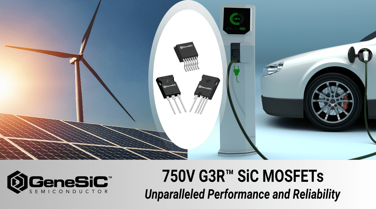
G3R™ 750V SiC MOSFETs Offer Unparalleled Performance and Reliability

750V G3R SiC MOSFET

DULLES, VA, June 04, 2021 — GeneSiC’s next-generation 750V G3R™SiC MOSFETs will deliver unprecedented levels of performance, robustness and quality that exceeds its counterparts. System benefits include low on-state drops at operating temperatures, faster switching speeds, increased power density, minimal ringing (low EMI) and compact system size. GeneSiC’s G3R™, offered in optimized low-inductance discrete packages (SMD and through hole), are optimized to operate with lowest power losses under all operating conditions and ultra-fast switching speeds. These devices have substantially better performance levels as compared to contemporary SiC MOSFETs.

750V G3R SiC MOSFET

“High-efficiency energy usage has become a critical deliverable in next-generation power converters and SiC power devices continue to be the key components driving this revolution. After years of development work towards achieving the lowest on-state resistance and robust short circuit and avalanche performance, we are excited to release the industry’s best performing 750V SiC MOSFETs. Our G3R™ enable power electronics designers to meet the challenging efficiency, power density and quality goals in applications like solar inverters, EV on-board chargers and server/telecom power supplies. An assured quality, supported by fast turn-around and automotive-qualified high volume manufacturing further enhances their value proposition. ” said Dr. Ranbir Singh, President at GeneSiC Semiconductor.

Features –

  • Industry’s lowest gate charge (QG) and internal gate resistance (RG(INT))
  • Lowest RDS(ON) change with temperature
  • Low output capacitance (COSS) and miler capacitance (CGD)
  • 100% avalanche (UIL) tested during production
  • Industry-leading short circuit withstand capability
  • Fast and reliable body diode with low VF and low QRR
  • High and stable gate threshold voltage (VTH) across all temperature and drain-bias conditions
  • Advanced packaging technology for lower thermal resistance and lower ringing
  • Manufacturing uniformity of RDS(ON), VTH and breakdown voltage (BV)
  • Comprehensive product portfolio and safer supply chain with automotive-qualified high volume manufacturing

Applications –

  • Solar (PV) Inverters
  • EV / HEV Onboard Chargers
  • Server & Telecom Power Supplies
  • Uninterruptible Power Supplies (UPS)
  • DC-DC Converters
  • Switched Mode Power Supplies (SMPS)
  • Energy Storage and Battery Charging
  • Induction Heating

All of GeneSiC Semiconductor’s SiC MOSFETs are targeted for automotive applications (AEC-Q101) and PPAP-capable.

G3R60MT07J – 750V 60mΩ TO-263-7 G3R&trade SiC MOSFET

G3R60MT07K – 750V 60mΩ TO-247-4 G3R&trade SiC MOSFET

G3R60MT07D – 750V 60mΩ TO-247-3 G3R&trade SiC MOSFET

For datasheet and other resources, visit – www.genesicsemi.com/sic-mosfet/ or contact sales@genesicsemi.com

All devices are available for purchase through authorized distributors – www.genesicsemi.com/sales-support

Digi-Key Electronics

Newark Farnell element14

Mouser Electronics

Arrow Electronics

About GeneSiC Semiconductor, Inc.

GeneSiC Semiconductor is a pioneer and world leader in Silicon Carbide technology, while also invested in high power Silicon technologies. The global leading manufacturers of industrial and defense systems depend on GeneSiC’s technology to elevate the performance and efficiency of their products. GeneSiC’s electronic components run cooler, faster, and more economically, and play a key role in conserving energy in a wide array of high power systems. We hold leading patents on wide band gap power device technologies; a market that is projected to reach more than $1 billion by 2022. Our core competency is to add more value to our customers’ end product. Our performance and cost metrics are setting standards in the Silicon Carbide industry.

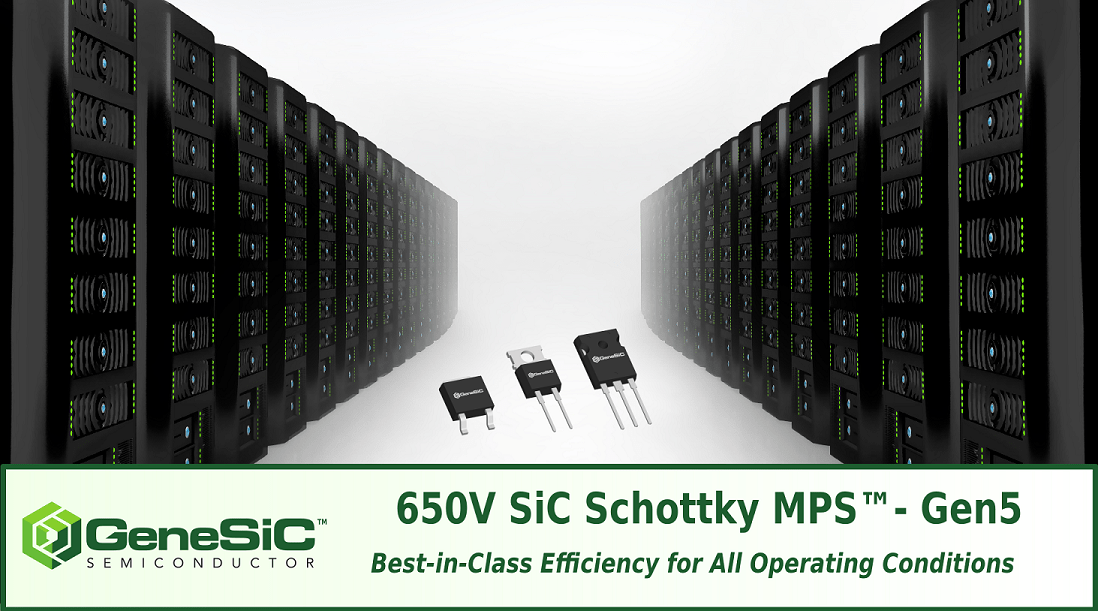
5th Generation 650V SiC Schottky MPS™ Diodes for Best-in-Class Efficiency

Gen5 650V SiC Schottky MPS™

DULLES, VA, May 28, 2021 — GeneSiC Semiconductor, a pioneer and global supplier of Silicon Carbide (SiC) power semiconductor devices, announces the availability of 5th generation (GE*** series) SiC Schottky MPS™ rectifiers that are setting up a new benchmark with their superior price-performance index, industry-leading surge current and avalanche robustness, and high quality manufacturing.

“GeneSiC was one of the first SiC manufacturers to commercially supply SiC Schottky rectifiers in 2011. After more than a decade of supplying high-performance and high-quality SiC rectifiers in the industry, we are excited to release our 5th generation of SiC Schottky MPS™ (Merged-PiN-Schottky) diodes that offer industry-leading performance in all aspects to meet the high efficiency and power density goals in applications like server/telecom power supplies and battery chargers. The revolutionary feature that makes our 5th Generation (GE*** series) SiC Schottky MPS™ diodes stand out among its peers is the low built-in voltage (also known as knee-voltage);it enables lowest diode conduction losses at all load conditions – crucial for applications demanding high-efficiency energy usage. In contrast to other competitor SiC diodes also designed to offer low-knee characteristics, an additional feature of our Gen5 diode designs is that they still maintain that high level of avalanche (UIL) ruggedness that our customers have come to expect from GeneSiC’s Gen3 (GC*** series) and Gen4 (GD*** series) SiC Schottky MPS™” said Dr. Siddarth Sundaresan, Vice President of Technology at GeneSiC Semiconductor.

Features –

  • Low Built-In Voltage – Lowest Conduction Losses for All Load Conditions
  • Superior Figure of Merit – QC x VF
  • Optimal Price Performance
  • Enhanced Surge Current Capability
  • 100% Avalanche (UIL) Tested
  • Low Thermal Resistance for Cooler Operation
  • Zero Forward and Reverse Recovery
  • Temperature Independent Fast Switching
  • Positive Temperature Coefficient of VF

Applications –

  • Boost Diode in Power Factor Correction (PFC)
  • Server and Telecom Power Supplies
  • Solar Inverters
  • Uninterruptible Power Supplies (UPS)
  • Battery Chargers
  • Freewheeling / Anti-parallel Diode in Inverters

GE04MPS06E – 650V 4A TO-252-2 SiC Schottky MPS™

GE06MPS06E – 650V 6A TO-252-2 SiC Schottky MPS™

GE08MPS06E – 650V 8A TO-252-2 SiC Schottky MPS™

GE10MPS06E – 650V 10A TO-252-2 SiC Schottky MPS™

GE04MPS06A – 650V 4A TO-220-2 SiC Schottky MPS™

GE06MPS06A – 650V 6A TO-220-2 SiC Schottky MPS™

GE08MPS06A – 650V 8A TO-220-2 SiC Schottky MPS™

GE10MPS06A – 650V 10A TO-220-2 SiC Schottky MPS™

GE12MPS06A – 650V 12A TO-220-2 SiC Schottky MPS™

GE2X8MPS06D – 650V 2x8A TO-247-3 SiC Schottky MPS™

GE2X10MPS06D – 650V 2x10A TO-247-3 SiC Schottky MPS™

All devices are available for purchase through authorized distributors – www.genesicsemi.com/sales-support

For datasheet and other resources, visit – www.genesicsemi.com/sic-schottky-mps/ or contact sales@genesicsemi.com

About GeneSiC Semiconductor, Inc.

GeneSiC Semiconductor is a pioneer and world leader in Silicon Carbide technology, while also invested in high power Silicon technologies. The global leading manufacturers of industrial and defense systems depend on GeneSiC’s technology to elevate the performance and efficiency of their products. GeneSiC’s electronic components run cooler, faster, and more economically, and play a key role in conserving energy in a wide array of high power systems. We hold leading patents on wide band gap power device technologies; a market that is projected to reach more than $1 billion by 2022. Our core competency is to add more value to our customers’ end product. Our performance and cost metrics are setting standards in the Silicon Carbide industry.

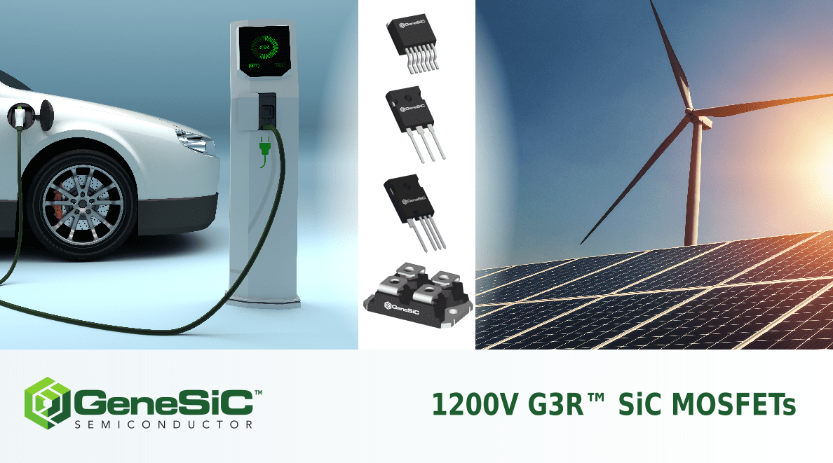
GeneSiC’s New 3rd Generation SiC MOSFETs Featuring the Industry’s Best Figure-of-Merits

DULLES, VA, February 12, 2020 — GeneSiC Semiconductor’s next-generation 1200V G3R™SiC MOSFETs with RDS(ON) levels ranging from 20 mΩ to 350 mΩ deliver unprecedented levels of performance, robustness and quality that exceeds its counterparts. System benefits include higher efficiency, faster switching frequency, increased power density, reduced ringing (EMI) and compact system size.

GeneSiC announces the availability of its industry-leading 3rd generation Silicon Carbide MOSFETs that feature industry-leading performance, robustness and quality to harness never before seen levels of efficiency and system reliability in automotive and industrial applications.

These G3R™ SiC MOSFETs, offered in optimized low-inductance discrete packages (SMD and through hole), are highly optimized for power system designs requiring elevated efficiency levels and ultra-fast switching speeds. These devices have substantially better performance levels as compared to competing products. An assured quality, supported by fast turn-around high volume manufacturing further enhances their value proposition.

“After years of development work towards achieving the lowest on-state resistance and enhanced short circuit performance, we are excited to release the industry’s best performing 1200V SiC MOSFETs with over 15+ discrete and bare chip products. If the next-generation power electronics systems are to meet the challenging efficiency, power density and quality goals in applications like automotive, industrial, renewable energy, transportation, IT and telecom, then they require significantly improved device performance and reliability as compared to presently available SiC MOSFETs” said Dr. Ranbir Singh, President at GeneSiC Semiconductor.

Features –

  • Superior QG x RDS(ON) figure-of-merit – G3R™ SiC MOSFETs feature the industry’s lowest on-state resistance with a very low gate charge, resulting in to 20% better figure-of-merit than any other similar competitor device
  • Low conduction losses at all temperatures – GeneSiC’s MOSFETs feature the softest temperature dependence of on-state resistance to offer very low conduction losses at all temperatures; significantly better than any other trench and planar SiC MOSFETs in the market
  • 100 % avalanche tested – Robust UIL capability is a critical requirement for the majority of field applications. GeneSiC’s 1200V SiC MOSFET discrete are 100 % avalanche (UIL) tested during production
  • Low gate charge and low internal gate resistance – These parameters are critical towards realizing ultra-fast switching and achieving highest efficiencies (low Eon -Eoff) across a wide range of application switching frequencies
  • Normally-off stable operation up to 175°C – All of GeneSiC’s SiC MOSFETs are designed and fabricated with state-of-the-art processes to deliver products that are stable and reliable at all operating conditions without any malfunction risk. The superior gate oxide quality of these devices prevents any threshold (VTH) drift
  • Low device capacitances – G3R™ are designed to drive faster and more efficient with their low device capacitances – Ciss, Coss and Crss
  • Fast and reliable body diode with low intrinsic charge – GeneSiC’s MOSFETs feature benchmark low reverse recovery charge (QRR) at all temperatures; 30% better than any similarly rated competitor device. This offers further reduction in power losses and boosts operating frequencies
  • Ease of use – G3R™ SiC MOSFETs are designed to be driven at +15V / -5V gate drive. This offers broadest compatibility with existing commercial IGBT and SiC MOSFET gate drivers

Applications –

  • Electric Vehicle – Power Train and Charging
  • Solar Inverter and Energy Storage
  • Industrial Motor Drive
  • Uninterruptible Power Supply (UPS)
  • Switched Mode Power Supply (SMPS)
  • Bi-directional DC-DC converters
  • Smart Grid and HVDC
  • Induction Heating and Welding
  • Pulsed Power Application

All devices are available for purchase through authorized distributors – www.genesicsemi.com/sales-support

Digi-Key Electronics

Newark Farnell element14

Mouser Electronics

Arrow Electronics

For datasheet and other resources, visit – www.genesicsemi.com/sic-mosfet or contact sales@genesicsemi.com

All of GeneSiC Semiconductor’s SiC MOSFETs are targeted for automotive applications (AEC-Q101) and PPAP-capable. All devices are offered in industry standard D2PAK, TO-247 and SOT-227 packages.

About GeneSiC Semiconductor, Inc.

GeneSiC Semiconductor is a pioneer and world leader in Silicon Carbide technology, while also invested in high power Silicon technologies. The global leading manufacturers of industrial and defense systems depend on GeneSiC’s technology to elevate the performance and efficiency of their products. GeneSiC’s electronic components run cooler, faster, and more economically, and play a key role in conserving energy in a wide array of high power systems. We hold leading patents on wide band gap power device technologies; a market that is projected to reach more than $1 billion by 2022. Our core competency is to add more value to our customers’ end product. Our performance and cost metrics are setting standards in the Silicon Carbide industry.

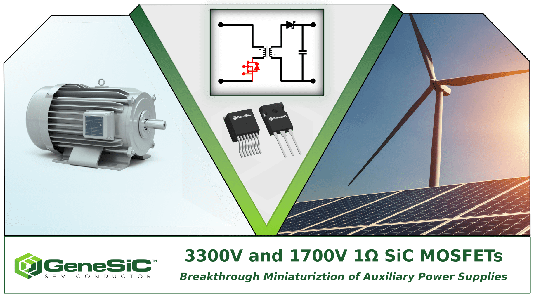
GeneSiC’s 3300V and 1700V 1000mΩ SiC MOSFETs Revolutionize the Miniaturization of Auxiliary Power Supplies

DULLES, VA, December 4, 2020 — GeneSiC announces availability of industry-leading 3300V and 1700V discrete SiC MOSFETs that are optimized to achieve unparalleled miniaturization, reliability and energy savings in industrial housekeeping power.

GeneSiC Semiconductor, a pioneer and global supplier of a comprehensive portfolio of Silicon Carbide (SiC) power semiconductors, today announces the immediate availability of next-generation 3300V and 1700V 1000mΩ SiC MOSFETs – G2R1000MT17J, G2R1000MT17D, and G2R1000MT33J. These SiC MOSFETs enable superior performance levels, based on flagship Figures of Merit (FoM) that enhance and simplify power systems across energy storage, renewable energy, industrial motors, general-purpose inverters and industrial lighting. Products released are:

G2R1000MT33J – 3300V 1000mΩ TO-263-7 SiC MOSFET

G2R1000MT17D – 1700V 1000mΩ TO-247-3 SiC MOSFET

G2R1000MT17J – 1700V 1000mΩ TO-263-7 SiC MOSFET

G3R450MT17D – 1700V 450mΩ TO-247-3 SiC MOSFET

G3R450MT17J – 1700V 450mΩ TO-263-7 SiC MOSFET

GeneSiC’s new 3300V and 1700V SiC MOSFETs, available in 1000mΩ and 450mΩ options as SMD and Through-Hole discrete packages, are highly optimized for power system designs requiring elevated efficiency levels and ultra-fast switching speeds. These devices have substantially better performance levels as compared to competing products. An assured quality, supported by fast turn-around high volume manufacturing further enhance their value proposition.

“In applications like 1500V solar inverters, the MOSFET in auxiliary power supply may have to withstand voltages in the range of 2500V, depending on the input voltage, turns ratio of the transformer and the output voltage. High breakdown voltage MOSFETs obviate the need for series connected switches in Flyback, Boost and Forward converters thereby reducing parts-count and reducing circuit complexity. GeneSiC’s 3300V and 1700V discrete SiC MOSFETs allow the designers to use simpler single switch based topology and at the same time provide customers with reliable, compact and cost-effective system” said Sumit Jadav, Senior Applications Manager at GeneSiC Semiconductor.

Features –

  • Superior price-performance index
  • Flagship QG x RDS(ON) figure of merit
  • Low intrinsic capacitance and low gate charge
  • Low losses at all temperatures
  • High avalanche and short circuit ruggedness
  • Benchmark threshold voltage for normally-off stable operation up to 175°C

Applications –

  • Renewable energy (solar inverters) and energy storage
  • Industrial motors (AC servos)
  • General-purpose inverters
  • Industrial lighting
  • Piezo drivers
  • Ion-beam generators

All devices are available for purchase through authorized distributors – www.genesicsemi.com/sales-support

For datasheet and other resources, visit – www.genesicsemi.com/sic-mosfet or contact sales@genesicsemi.com

About GeneSiC Semiconductor, Inc.

GeneSiC Semiconductor is a pioneer and world leader in Silicon Carbide technology, while also invested in high power Silicon technologies. The global leading manufacturers of industrial and defense systems depend on GeneSiC’s technology to elevate the performance and efficiency of their products. GeneSiC’s electronic components run cooler, faster, and more economically, and play a key role in conserving energy in a wide array of high power systems. We hold leading patents on wide band gap power device technologies; a market that is projected to reach more than $1 billion by 2022. Our core competency is to add more value to our customers’ end product. Our performance and cost metrics are setting standards in the Silicon Carbide industry.

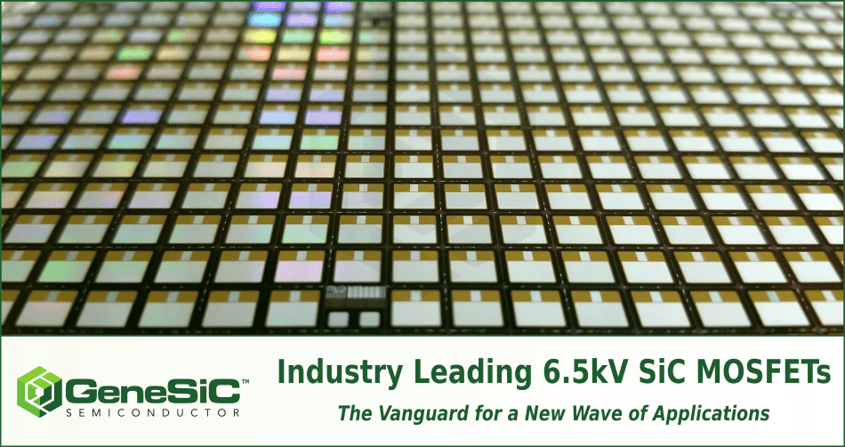
GeneSiC’s Industry Leading 6.5kV SiC MOSFETs – the Vanguard for a New Wave of Applications

6.5kV SiC MOSFETs

DULLES, VA, October 20, 2020 — GeneSiC’s releases 6.5kV silicon carbide MOSFETs to lead the forefront in delivering unprecedented levels of performance, efficiency and reliability in medium-voltage power conversion applications such as traction, pulsed power and smart grid infrastructure.

GeneSiC Semiconductor, a pioneer and global supplier of a broad range of Silicon Carbide (SiC) power semiconductors, today announces the immediate availability of 6.5kV SiC MOSFET bare chips – G2R300MT65-CAL and G2R325MS65-CAL. Full SiC modules utilizing this technology are soon to be released. Applications are expected to include traction, pulsed power, smart grid infrastructure and other medium-voltage power converters.

G2R300MT65-CAL – 6.5kV 300mΩ G2R™ SiC MOSFET Bare Chip

G2R325MS65-CAL – 6.5kV 325mΩ G2R™ SiC MOSFET (with Integrated-Schottky) Bare Chip

G2R100MT65-CAL – 6.5kV 100mΩ G2R™ SiC MOSFET Bare Chip

GeneSiC’s innovation features a SiC double-implanted metal oxide semiconductor (DMOSFET) device structure with a junction barrier schottky (JBS) rectifier integrated into the SiC DMOSFET unit cell. This leading-edge power device can be used in a variety of power conversion circuits in the next generation of power conversion systems. Other significant advantages include more efficient bi-directional performance, temperature independent switching, low switching and conduction losses, reduced cooling requirements, superior long-term reliability, ease of paralleling devices and cost benefits. GeneSiC’s technology offers superior performance and also has the potential to reduce the net SiC material footprint in power converters.

“GeneSiC’s 6.5kV SiC MOSFETs are designed and fabricated on 6-inch wafers to realize low on-state resistance, highest quality, and superior price-performance index. This next-generation MOSFETs technology promises exemplar performance, superior ruggedness and long-term reliability in medium-voltage power conversion applications.” said Dr. Siddarth Sundaresan, VP of Technology at GeneSiC Semiconductor.

GeneSiC’s 6.5kV G2R™ SiC MOSFET technology features –

  • High avalanche (UIS) and short circuit ruggedness
  • Superior QG x RDS(ON) figure of merit
  • Temperature independent switching losses
  • Low capacitances and low gate charge
  • Low losses at all temperatures
  • Normally-off stable operation up to 175°C
  • +20 V / -5 V gate drive

For datasheet and other resources, visit – www.genesicsemi.com/sic-mosfet/bare-chip or contact sales@genesicsemi.com

About GeneSiC Semiconductor, Inc.

GeneSiC Semiconductor is a pioneer and world leader in Silicon Carbide technology, while also invested in high power Silicon technologies. The global leading manufacturers of industrial and defense systems depend on GeneSiC’s technology to elevate the performance and efficiency of their products. GeneSiC’s electronic components run cooler, faster, and more economically, and play a key role in conserving energy in a wide array of high power systems. We hold leading patents on wide band gap power device technologies; a market that is projected to reach more than $1 billion by 2022. Our core competency is to add more value to our customers’ end product. Our performance and cost metrics are setting standards in the Silicon Carbide industry.

GeneSiC wins the prestigious R&D100 Award for SiC-Based Monolithic Transistor-Rectifier Switch

DULLES, VA, December 5, 2019 — R&D Magazine has selected GeneSiC Semiconductor Inc. of Dulles, VA as a recipient of the prestigious 2019 R&D 100 Award for development of SiC-Based Monolithic Transistor-Rectifier Switch.

GeneSiC Semiconductor Inc, a key innovator in the Silicon Carbide based power devices was honored with the announcement that it has been awarded the prestigious 2019 R&D 100 Award. This award recognizes GeneSiC for introducing one of the most significant, newly introduced research and development advances among multiple disciplines during 2018. R&D Magazine recognized GeneSiC’s medium voltage SiC power device technology for its ability to monolithically integrate MOSFET and Schottky rectifier on a single chip. These capabilities achieved by GeneSiC’s device critically enable power electronics researchers to develop next-generation power electronic systems like inverters and DC-DC converters. This will allow product developments within electric vehicles, charging infrastructure, renewable energy and energy storage industries. GeneSiC has booked orders from multiple customers towards demonstration of advanced power electronics hardware using these devices and continues to develop its family of Silicon Carbide MOSFET products. The R&D on early version for power conversion applications were developed through US Dept. of Energy and collaboration with Sandia National Laboratories.

The annual technology competition run by R&D Magazine evaluated entries from various companies and industry players, research organizations and universities around the world. The magazine’s editors and a panel of outside experts served as judges, evaluating each entry in terms of its importance to the world of science and research.

According to R&D Magazine, winning an R&D 100 Award provides a mark of excellence known to industry, government, and academia as proof that the product is one of the most innovative ideas of the year. This award recognizes GeneSiC as a global leader in the creation of technology-based products that make a difference in how we work and live.

About GeneSiC Semiconductor, Inc.

GeneSiC is a fast emerging innovator in the area of SiC power devices and has a strong commitment to the development of Silicon Carbide (SiC) based devices for: (a) HV-HF SiC devices for Power Grid, Pulsed power and Directed Energy Weapons; and (b) High temperature SiC power devices for aircraft actuators and oil exploration. GeneSiC Semiconductor Inc. develops Silicon Carbide (SiC) based semiconductor devices for high temperature, radiation, and power grid applications. This includes development of rectifiers, FETs, bipolar devices as well as particle & photonic detectors. GeneSiC has access to an extensive suite of semiconductor design, fabrication, characterization and testing facilities for such devices. GeneSiC capitalizes on its core competency in device and process design to develop the best possible SiC devices for its customers. The company distinguishes itself by providing high quality products that are specifically tuned to each customer’s requirements. GeneSiC has prime/sub-contracts from major US Government agencies including ARPA-E, US Dept of Energy, Navy, DARPA, Dept of Homeland Security, Dept of Commerce and other departments within the US Dept. of Defense. GeneSiC continues to rapidly enhance the equipment and personnel infrastructure at its Dulles, Virginia facility. The company is aggressively hiring personnel experienced in compound semiconductor device fabrication, semiconductor testing and detector designs. Additional information about the company and its products may be obtained by calling GeneSiC at 703-996-8200 or by visiting www.genesicsemi.com.

High-current capable 650V, 1200V and 1700V SiC Schottky MPS™ diodes in mini-module SOT-227 package

DULLES, VA, May 11, 2019 — GeneSiC becomes a market leader in high-current capable (100 A and 200 A) SiC schottky diodes in SOT-227 mini-module

GeneSiC has introduced GB2X50MPS17-227, GC2X50MPS06-227 and GC2X100MPS06-227; the industry’s highest current rated 650V and 1700V SiC schottky diodes, adding to the existing 1200V SiC schottky diode mini-module portfolio – GB2X50MPS12-227 and GB2X100MPS12-227. These SiC diodes replace silicon-based ultra-fast recovery diodes, enabling engineers to build switching circuits with greater efficiency and higher power density. Applications are expected to include electric vehicle fast chargers, motor drives, transportation power supplies, high power rectification and industrial power supplies.

In addition to the isolated base-plate of the SOT-227 mini-module package, these newly released diodes feature low forward voltage drop, zero forward recovery, zero reverse recovery, low junction capacitance and are rated for a maximum operating temperature of 175°C. GeneSiC’s third generation SiC schottky diode technology provides industry leading avalanche ruggedness and surge current (Ifsm) robustness, combined with high quality automotive qualified 6-inch fabrication and advanced high reliability discrete assembly technology.

These SiC diodes are pin-compatible direct replacements to other diodes available in the SOT-227 (mini-module) package. Benefitting from their lower power losses (cooler operation) and high frequency switching capability, designers can now achieve greater conversion efficiency and greater power density in designs.

About GeneSiC Semiconductor, Inc.

GeneSiC is a fast emerging innovator in the area of SiC power devices and has a strong commitment to the development of Silicon Carbide (SiC) based devices for: (a) HV-HF SiC devices for Power Grid, Pulsed power and Directed Energy Weapons; and (b) High temperature SiC power devices for aircraft actuators and oil exploration. GeneSiC Semiconductor Inc. develops Silicon Carbide (SiC) based semiconductor devices for high temperature, radiation, and power grid applications. This includes development of rectifiers, FETs, bipolar devices as well as particle & photonic detectors. GeneSiC has access to an extensive suite of semiconductor design, fabrication, characterization and testing facilities for such devices. GeneSiC capitalizes on its core competency in device and process design to develop the best possible SiC devices for its customers. The company distinguishes itself by providing high quality products that are specifically tuned to each customer’s requirements. GeneSiC has prime/sub-contracts from major US Government agencies including ARPA-E, US Dept of Energy, Navy, DARPA, Dept of Homeland Security, Dept of Commerce and other departments within the US Dept. of Defense. GeneSiC continues to rapidly enhance the equipment and personnel infrastructure at its Dulles, Virginia facility. The company is aggressively hiring personnel experienced in compound semiconductor device fabrication, semiconductor testing and detector designs. Additional information about the company and its products may be obtained by calling GeneSiC at 703-996-8200 or by visiting www.genesicsemi.com.

GeneSiC releases industry’s best performing 1700V SiC Schottky MPS™ diodes

DULLES, VA, January 7, 2019 — GeneSiC releases a comprehensive portfolio of its third generation 1700V SiC Schottky MPS™ diodes in TO-247-2 package

GeneSiC has introduced GB05MPS17-247, GB10MPS17-247, GB25MPS17-247 and GB50MPS17-247; the industry’s best performing 1700V SiC diodes available in the popular TO-247-2 through-hole package. These 1700V SiC diodes replace silicon-based ultra-fast recovery diodes and other old generation 1700V SiC JBS, enabling engineers to build switching circuits with greater efficiency and higher power density. Applications are expected to include electric vehicle fast chargers, motor drives, transportation power supplies and renewable energy.

GB50MPS17-247 is a 1700V 50A SiC merged-PiN-schottky diode, the industry’s highest current rated discrete SiC power diode. These newly released diodes feature low forward voltage drop, zero forward recovery, zero reverse recovery, low junction capacitance and are rated for a maximum operating temperature of 175°C. GeneSiC’s third generation SiC schottky diode technology provides industry leading avalanche ruggedness and surge current (Ifsm) robustness, combined with high quality automotive qualified 6-inch foundry and advanced high reliability discrete assembly technology.

These SiC diodes are pin-compatible direct replacements to other diodes available in the TO-247-2 package. Benefitting from their lower power losses (cooler operation) and high frequency switching capability, designers can now achieve greater conversion efficiency and greater power density in designs.

About GeneSiC Semiconductor, Inc.

GeneSiC is a fast emerging innovator in the area of SiC power devices and has a strong commitment to the development of Silicon Carbide (SiC) based devices for: (a) HV-HF SiC devices for Power Grid, Pulsed power and Directed Energy Weapons; and (b) High temperature SiC power devices for aircraft actuators and oil exploration. GeneSiC Semiconductor Inc. develops Silicon Carbide (SiC) based semiconductor devices for high temperature, radiation, and power grid applications. This includes development of rectifiers, FETs, bipolar devices as well as particle & photonic detectors. GeneSiC has access to an extensive suite of semiconductor design, fabrication, characterization and testing facilities for such devices. GeneSiC capitalizes on its core competency in device and process design to develop the best possible SiC devices for its customers. The company distinguishes itself by providing high quality products that are specifically tuned to each customer’s requirements. GeneSiC has prime/sub-contracts from major US Government agencies including ARPA-E, US Dept of Energy, Navy, DARPA, Dept of Homeland Security, Dept of Commerce and other departments within the US Dept. of Defense. GeneSiC continues to rapidly enhance the equipment and personnel infrastructure at its Dulles, Virginia facility. The company is aggressively hiring personnel experienced in compound semiconductor device fabrication, semiconductor testing and detector designs. Additional information about the company and its products may be obtained by calling GeneSiC at 703-996-8200 or by visiting www.genesicsemi.com.

GeneSiC Interviewed at PCIM 2016 in Nuremberg, Germany

Power System Design Interviews GeneSiC

Nuremberg, Germany May 12, 2016 — GeneSiC Semiconductor’s President was interviewed by Alix Paultre of Power Systems Design (https://www.powersystemsdesign.com/psdcast-ranbir-singh-of-genesic-on-their-latest-silicon-carbide-tech/67) at the PCIM show in Nuremberg, Germany.