GeneSiC’s Industry Leading 6.5kV SiC MOSFETs – the Vanguard for a New Wave of Applications

6.5kV SiC MOSFETs

DULLES, VA, October 20, 2020 — GeneSiC’s releases 6.5kV silicon carbide MOSFETs to lead the forefront in delivering unprecedented levels of performance, efficiency and reliability in medium-voltage power conversion applications such as traction, pulsed power and smart grid infrastructure.

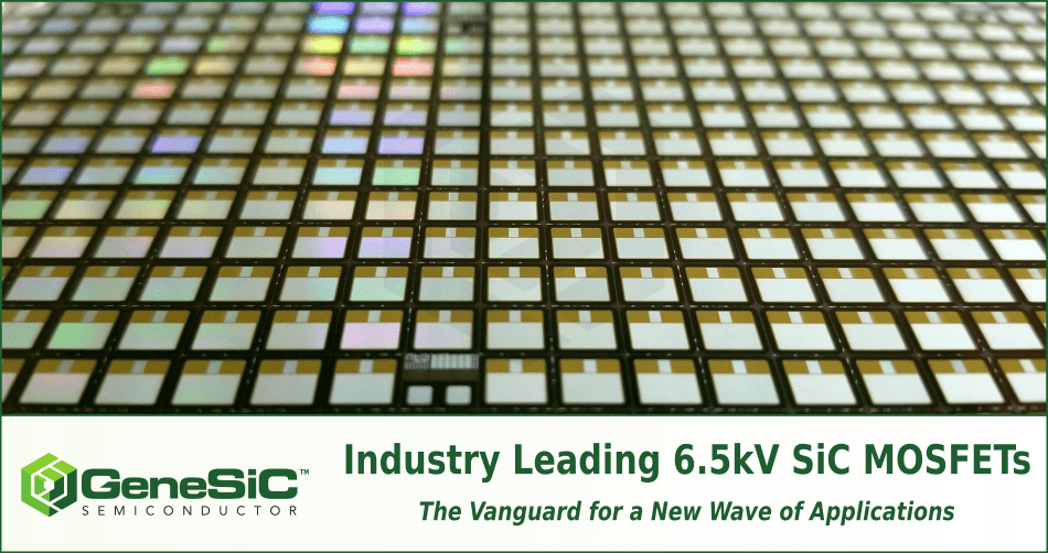
GeneSiC Semiconductor, a pioneer and global supplier of a broad range of Silicon Carbide (SiC) power semiconductors, today announces the immediate availability of 6.5kV SiC MOSFET bare chips – G2R300MT65-CAL and G2R325MS65-CAL. Full SiC modules utilizing this technology are soon to be released. Applications are expected to include traction, pulsed power, smart grid infrastructure and other medium-voltage power converters.

G2R300MT65-CAL – 6.5kV 300mΩ G2R™ SiC MOSFET Bare Chip

G2R325MS65-CAL – 6.5kV 325mΩ G2R™ SiC MOSFET (with Integrated-Schottky) Bare Chip

G2R100MT65-CAL – 6.5kV 100mΩ G2R™ SiC MOSFET Bare Chip

GeneSiC’s innovation features a SiC double-implanted metal oxide semiconductor (DMOSFET) device structure with a junction barrier schottky (JBS) rectifier integrated into the SiC DMOSFET unit cell. This leading-edge power device can be used in a variety of power conversion circuits in the next generation of power conversion systems. Other significant advantages include more efficient bi-directional performance, temperature independent switching, low switching and conduction losses, reduced cooling requirements, superior long-term reliability, ease of paralleling devices and cost benefits. GeneSiC’s technology offers superior performance and also has the potential to reduce the net SiC material footprint in power converters.

“GeneSiC’s 6.5kV SiC MOSFETs are designed and fabricated on 6-inch wafers to realize low on-state resistance, highest quality, and superior price-performance index. This next-generation MOSFETs technology promises exemplar performance, superior ruggedness and long-term reliability in medium-voltage power conversion applications.” said Dr. Siddarth Sundaresan, VP of Technology at GeneSiC Semiconductor.

GeneSiC’s 6.5kV G2R™ SiC MOSFET technology features –

  • High avalanche (UIS) and short circuit ruggedness
  • Superior QG x RDS(ON) figure of merit
  • Temperature independent switching losses
  • Low capacitances and low gate charge
  • Low losses at all temperatures
  • Normally-off stable operation up to 175°C
  • +20 V / -5 V gate drive

For datasheet and other resources, visit – www.genesicsemi.com/sic-mosfet/bare-chip or contact sales@genesicsemi.com

About GeneSiC Semiconductor, Inc.

GeneSiC Semiconductor is a pioneer and world leader in Silicon Carbide technology, while also invested in high power Silicon technologies. The global leading manufacturers of industrial and defense systems depend on GeneSiC’s technology to elevate the performance and efficiency of their products. GeneSiC’s electronic components run cooler, faster, and more economically, and play a key role in conserving energy in a wide array of high power systems. We hold leading patents on wide band gap power device technologies; a market that is projected to reach more than $1 billion by 2022. Our core competency is to add more value to our customers’ end product. Our performance and cost metrics are setting standards in the Silicon Carbide industry.

GeneSiC wins $2.53M from ARPA-E towards development of Silicon Carbide Thyristor-based devices

DULLES, VA, September 28, 2010 – Advanced Research Projects Agency – Energy (ARPA-E) has entered into a Cooperative Agreement with the GeneSiC Semiconductor-led team towards the development of the novel ultra high-voltage silicon carbide (SiC) Thyristor based devices. These devices are expected to be key enablers for integrating large-scale wind and solar power plants into the next-generation Smart Grid.

“This highly competitive award to GeneSiC will allow us to extend our technical leadership position in the multi-kV Silicon Carbide technology, as well as our commitment to grid-scale alternative energy solutions with solid state solutions,” commented Dr. Ranbir Singh, President of GeneSiC. “Multi-kV SiC Thyristors we’re developing are the key enabling technology towards the realization of Flexible AC Transmission Systems (FACTS) elements and High Voltage DC (HVDC) architectures envisaged towards an integrated, efficient, Smart Grid of the future. GeneSiC’s SiC-based Thyristors offer 10X higher voltage, 100X faster switching frequencies and higher temperature operation in FACTS and HVDC power processing solutions as compared to conventional Silicon-based Thyristors.”

In April 2010, GeneSiC responded to the Agile Delivery of Electrical Power Technology (ADEPT) solicitation from ARPA-E that sought to invest in materials for fundamental advances in high voltage switches that has the potential to leapfrog existing power converter performance while offering reductions in cost. The company’s proposal titled “Silicon Carbide Anode Switched Thyristor for medium voltage power conversion” was selected to provide a lightweight, solid-state, medium voltage energy conversion for high power applications such as solid-state electrical substations and wind turbine generators. Deploying these advanced power semiconductor technologies could provide as much as a 25-30 percent reduction in electricity consumption through increased efficiencies in delivery of electrical power. Innovations selected were to support and promote U.S. businesses through technological leadership, through a highly competitive process.

Silicon carbide is a next-generation semiconductor material with vastly superior properties to conventional silicon, such as the ability to handle ten times the voltage—and one-hundred times the current—at temperatures as high as 300ºC. These characteristics make it ideally suited to high-power applications such as hybrid and electric vehicles, renewable energy (wind and solar) installations, and electrical-grid control systems.

It is now well established that ultra-high voltage (>10kV) Silicon Carbide (SiC) device technology will play a revolutionary role in the next-generation utility grid. Thyristor-based SiC devices offer the highest on-state performance for >5 kV devices, and are widely applicable towards medium voltage power conversion circuits like Fault-Current Limiters, AC-DC converters, Static VAR Compensators and Series Compensators. SiC based Thyristors also offer the best chance of early adoption due to their similarities to conventional power grid elements. Other promising applications and advantages for these devices include:

  • Power-management and power-conditioning systems for Medium Voltage DC conversion sought under Future Naval Capability (FNC) of US Navy, Electro-magnetic launch systems, high energy weapon systems and medical imaging. The 10-100X higher operating frequency capability allows unprecedented improvements in size, weight, volume and ultimately, cost of such systems.
  • A variety of energy storage, high-temperature and high-energy physics applications. Energy storage and power grid applications are receiving increasing attention as the world focuses on more efficient and cost-effective energy-management solutions.

GeneSiC is a fast emerging innovator in the area of SiC power devices and has a strong commitment to the development of Silicon Carbide (SiC) based devices for: (a) HV-HF SiC devices for Power Grid, Pulsed power and Directed Energy Weapons; and (b) High temperature SiC power devices for aircraft actuators and oil exploration.

“We’ve emerged as a leader in ultra-high voltage SiC technology by leveraging our core competency in device and process design with an extensive suite of fabrication, characterization, and test facilities,” concludes Dr. Singh. “GeneSiC’s position has now been effectively validated by the US DOE with this significant follow-on award.”

About GeneSiC Semiconductor

Strategically located near Washington, DC in Dulles, Virginia, GeneSiC Semiconductor Inc. is a leading innovator in high-temperature, high-power and ultra high-voltage silicon carbide (SiC) devices. Current development projects include high-temperature rectifiers, SuperJunction Transistors (SJT) and a wide variety of Thyristor based devices. GeneSiC has or has had prime/sub-contracts from major US Government agencies, including the Department of Energy, Navy, Army, DARPA, and the Department of Homeland Security. The company is currently experiencing substantial growth, and hiring qualified personnel in power-device and detector design, fabrication, and testing. To find out more, please visit www.genesicsemi.com.