G3R™ 750V SiC MOSFETs Offer Unparalleled Performance and Reliability

750V G3R SiC MOSFET

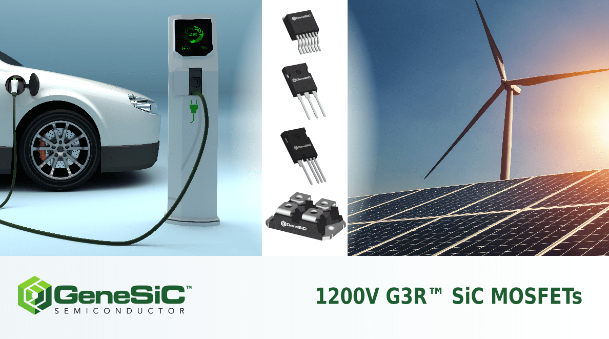
DULLES, VA, June 04, 2021 — GeneSiC’s next-generation 750V G3R™SiC MOSFETs will deliver unprecedented levels of performance, robustness and quality that exceeds its counterparts. System benefits include low on-state drops at operating temperatures, faster switching speeds, increased power density, minimal ringing (low EMI) and compact system size. GeneSiC’s G3R™, offered in optimized low-inductance discrete packages (SMD and through hole), are optimized to operate with lowest power losses under all operating conditions and ultra-fast switching speeds. These devices have substantially better performance levels as compared to contemporary SiC MOSFETs.

750V G3R SiC MOSFET

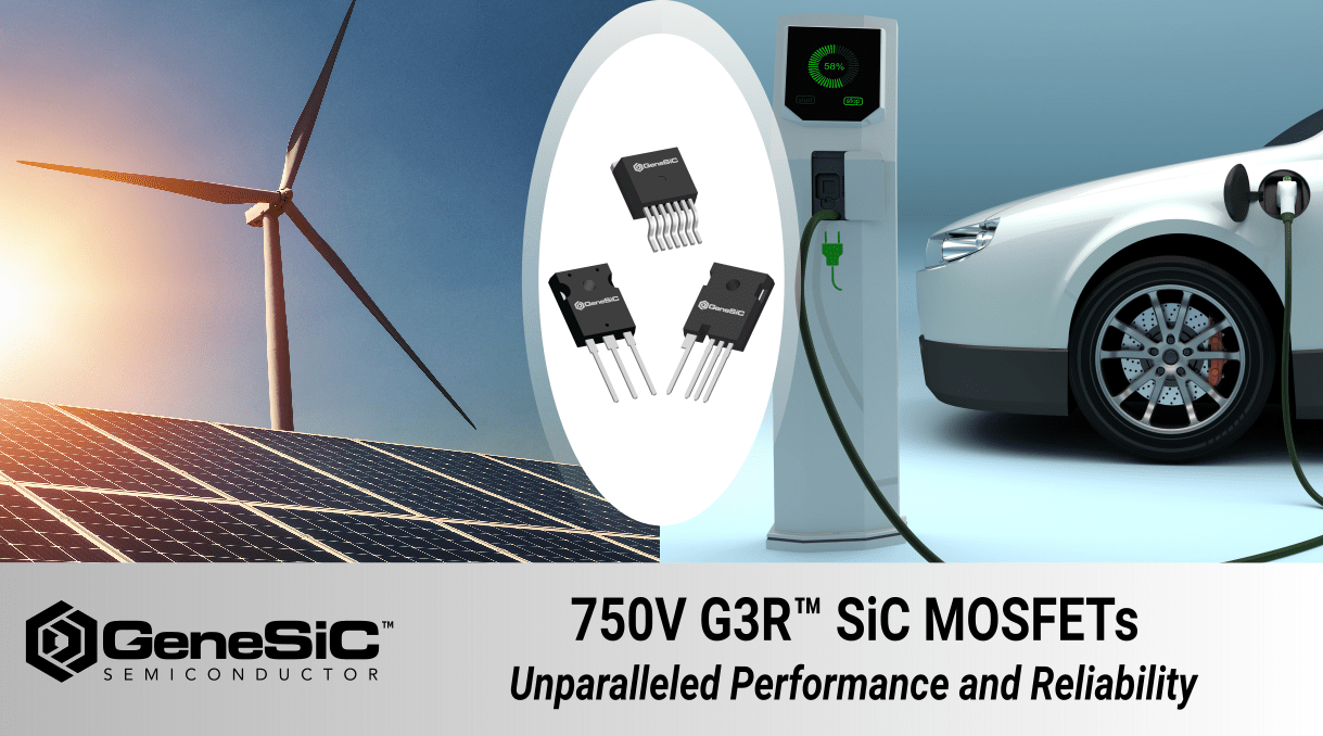
“High-efficiency energy usage has become a critical deliverable in next-generation power converters and SiC power devices continue to be the key components driving this revolution. After years of development work towards achieving the lowest on-state resistance and robust short circuit and avalanche performance, we are excited to release the industry’s best performing 750V SiC MOSFETs. Our G3R™ enable power electronics designers to meet the challenging efficiency, power density and quality goals in applications like solar inverters, EV on-board chargers and server/telecom power supplies. An assured quality, supported by fast turn-around and automotive-qualified high volume manufacturing further enhances their value proposition. ” said Dr. Ranbir Singh, President at GeneSiC Semiconductor.

Features –

  • Industry’s lowest gate charge (QG) and internal gate resistance (RG(INT))
  • Lowest RDS(ON) change with temperature
  • Low output capacitance (COSS) and miler capacitance (CGD)
  • 100% avalanche (UIL) tested during production
  • Industry-leading short circuit withstand capability
  • Fast and reliable body diode with low VF and low QRR
  • High and stable gate threshold voltage (VTH) across all temperature and drain-bias conditions
  • Advanced packaging technology for lower thermal resistance and lower ringing
  • Manufacturing uniformity of RDS(ON), VTH and breakdown voltage (BV)
  • Comprehensive product portfolio and safer supply chain with automotive-qualified high volume manufacturing
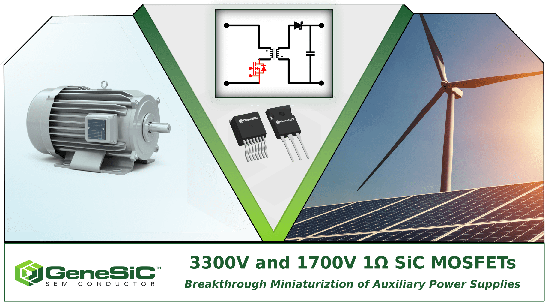
Applications –

  • Solar (PV) Inverters
  • EV / HEV Onboard Chargers
  • Server & Telecom Power Supplies
  • Uninterruptible Power Supplies (UPS)
  • DC-DC Converters
  • Switched Mode Power Supplies (SMPS)
  • Energy Storage and Battery Charging
  • Induction Heating

All of GeneSiC Semiconductor’s SiC MOSFETs are targeted for automotive applications (AEC-Q101) and PPAP-capable.

G3R60MT07J – 750V 60mΩ TO-263-7 G3R&trade SiC MOSFET

G3R60MT07K – 750V 60mΩ TO-247-4 G3R&trade SiC MOSFET

G3R60MT07D – 750V 60mΩ TO-247-3 G3R&trade SiC MOSFET

For datasheet and other resources, visit – www.genesicsemi.com/sic-mosfet/ or contact sales@genesicsemi.com

All devices are available for purchase through authorized distributors – www.genesicsemi.com/sales-support

Digi-Key Electronics

Newark Farnell element14

Mouser Electronics

Arrow Electronics

About GeneSiC Semiconductor, Inc.

GeneSiC Semiconductor is a pioneer and world leader in Silicon Carbide technology, while also invested in high power Silicon technologies. The global leading manufacturers of industrial and defense systems depend on GeneSiC’s technology to elevate the performance and efficiency of their products. GeneSiC’s electronic components run cooler, faster, and more economically, and play a key role in conserving energy in a wide array of high power systems. We hold leading patents on wide band gap power device technologies; a market that is projected to reach more than $1 billion by 2022. Our core competency is to add more value to our customers’ end product. Our performance and cost metrics are setting standards in the Silicon Carbide industry.

GeneSiC’s New 3rd Generation SiC MOSFETs Featuring the Industry’s Best Figure-of-Merits

DULLES, VA, February 12, 2020 — GeneSiC Semiconductor’s next-generation 1200V G3R™SiC MOSFETs with RDS(ON) levels ranging from 20 mΩ to 350 mΩ deliver unprecedented levels of performance, robustness and quality that exceeds its counterparts. System benefits include higher efficiency, faster switching frequency, increased power density, reduced ringing (EMI) and compact system size.

GeneSiC announces the availability of its industry-leading 3rd generation Silicon Carbide MOSFETs that feature industry-leading performance, robustness and quality to harness never before seen levels of efficiency and system reliability in automotive and industrial applications.

These G3R™ SiC MOSFETs, offered in optimized low-inductance discrete packages (SMD and through hole), are highly optimized for power system designs requiring elevated efficiency levels and ultra-fast switching speeds. These devices have substantially better performance levels as compared to competing products. An assured quality, supported by fast turn-around high volume manufacturing further enhances their value proposition.

“After years of development work towards achieving the lowest on-state resistance and enhanced short circuit performance, we are excited to release the industry’s best performing 1200V SiC MOSFETs with over 15+ discrete and bare chip products. If the next-generation power electronics systems are to meet the challenging efficiency, power density and quality goals in applications like automotive, industrial, renewable energy, transportation, IT and telecom, then they require significantly improved device performance and reliability as compared to presently available SiC MOSFETs” said Dr. Ranbir Singh, President at GeneSiC Semiconductor.

Features –

  • Superior QG x RDS(ON) figure-of-merit – G3R™ SiC MOSFETs feature the industry’s lowest on-state resistance with a very low gate charge, resulting in to 20% better figure-of-merit than any other similar competitor device
  • Low conduction losses at all temperatures – GeneSiC’s MOSFETs feature the softest temperature dependence of on-state resistance to offer very low conduction losses at all temperatures; significantly better than any other trench and planar SiC MOSFETs in the market
  • 100 % avalanche tested – Robust UIL capability is a critical requirement for the majority of field applications. GeneSiC’s 1200V SiC MOSFET discrete are 100 % avalanche (UIL) tested during production
  • Low gate charge and low internal gate resistance – These parameters are critical towards realizing ultra-fast switching and achieving highest efficiencies (low Eon -Eoff) across a wide range of application switching frequencies
  • Normally-off stable operation up to 175°C – All of GeneSiC’s SiC MOSFETs are designed and fabricated with state-of-the-art processes to deliver products that are stable and reliable at all operating conditions without any malfunction risk. The superior gate oxide quality of these devices prevents any threshold (VTH) drift
  • Low device capacitances – G3R™ are designed to drive faster and more efficient with their low device capacitances – Ciss, Coss and Crss
  • Fast and reliable body diode with low intrinsic charge – GeneSiC’s MOSFETs feature benchmark low reverse recovery charge (QRR) at all temperatures; 30% better than any similarly rated competitor device. This offers further reduction in power losses and boosts operating frequencies
  • Ease of use – G3R™ SiC MOSFETs are designed to be driven at +15V / -5V gate drive. This offers broadest compatibility with existing commercial IGBT and SiC MOSFET gate drivers

Applications –

  • Electric Vehicle – Power Train and Charging
  • Solar Inverter and Energy Storage
  • Industrial Motor Drive
  • Uninterruptible Power Supply (UPS)
  • Switched Mode Power Supply (SMPS)
  • Bi-directional DC-DC converters
  • Smart Grid and HVDC
  • Induction Heating and Welding
  • Pulsed Power Application

All devices are available for purchase through authorized distributors – www.genesicsemi.com/sales-support

Digi-Key Electronics

Newark Farnell element14

Mouser Electronics

Arrow Electronics

For datasheet and other resources, visit – www.genesicsemi.com/sic-mosfet or contact sales@genesicsemi.com

All of GeneSiC Semiconductor’s SiC MOSFETs are targeted for automotive applications (AEC-Q101) and PPAP-capable. All devices are offered in industry standard D2PAK, TO-247 and SOT-227 packages.

About GeneSiC Semiconductor, Inc.

GeneSiC Semiconductor is a pioneer and world leader in Silicon Carbide technology, while also invested in high power Silicon technologies. The global leading manufacturers of industrial and defense systems depend on GeneSiC’s technology to elevate the performance and efficiency of their products. GeneSiC’s electronic components run cooler, faster, and more economically, and play a key role in conserving energy in a wide array of high power systems. We hold leading patents on wide band gap power device technologies; a market that is projected to reach more than $1 billion by 2022. Our core competency is to add more value to our customers’ end product. Our performance and cost metrics are setting standards in the Silicon Carbide industry.

GeneSiC’s 3300V and 1700V 1000mΩ SiC MOSFETs Revolutionize the Miniaturization of Auxiliary Power Supplies

DULLES, VA, December 4, 2020 — GeneSiC announces availability of industry-leading 3300V and 1700V discrete SiC MOSFETs that are optimized to achieve unparalleled miniaturization, reliability and energy savings in industrial housekeeping power.

GeneSiC Semiconductor, a pioneer and global supplier of a comprehensive portfolio of Silicon Carbide (SiC) power semiconductors, today announces the immediate availability of next-generation 3300V and 1700V 1000mΩ SiC MOSFETs – G2R1000MT17J, G2R1000MT17D, and G2R1000MT33J. These SiC MOSFETs enable superior performance levels, based on flagship Figures of Merit (FoM) that enhance and simplify power systems across energy storage, renewable energy, industrial motors, general-purpose inverters and industrial lighting. Products released are:

G2R1000MT33J – 3300V 1000mΩ TO-263-7 SiC MOSFET

G2R1000MT17D – 1700V 1000mΩ TO-247-3 SiC MOSFET

G2R1000MT17J – 1700V 1000mΩ TO-263-7 SiC MOSFET

G3R450MT17D – 1700V 450mΩ TO-247-3 SiC MOSFET

G3R450MT17J – 1700V 450mΩ TO-263-7 SiC MOSFET

GeneSiC’s new 3300V and 1700V SiC MOSFETs, available in 1000mΩ and 450mΩ options as SMD and Through-Hole discrete packages, are highly optimized for power system designs requiring elevated efficiency levels and ultra-fast switching speeds. These devices have substantially better performance levels as compared to competing products. An assured quality, supported by fast turn-around high volume manufacturing further enhance their value proposition.

“In applications like 1500V solar inverters, the MOSFET in auxiliary power supply may have to withstand voltages in the range of 2500V, depending on the input voltage, turns ratio of the transformer and the output voltage. High breakdown voltage MOSFETs obviate the need for series connected switches in Flyback, Boost and Forward converters thereby reducing parts-count and reducing circuit complexity. GeneSiC’s 3300V and 1700V discrete SiC MOSFETs allow the designers to use simpler single switch based topology and at the same time provide customers with reliable, compact and cost-effective system” said Sumit Jadav, Senior Applications Manager at GeneSiC Semiconductor.

Features –

  • Superior price-performance index
  • Flagship QG x RDS(ON) figure of merit
  • Low intrinsic capacitance and low gate charge
  • Low losses at all temperatures
  • High avalanche and short circuit ruggedness
  • Benchmark threshold voltage for normally-off stable operation up to 175°C

Applications –

  • Renewable energy (solar inverters) and energy storage
  • Industrial motors (AC servos)
  • General-purpose inverters
  • Industrial lighting
  • Piezo drivers
  • Ion-beam generators

All devices are available for purchase through authorized distributors – www.genesicsemi.com/sales-support

For datasheet and other resources, visit – www.genesicsemi.com/sic-mosfet or contact sales@genesicsemi.com

About GeneSiC Semiconductor, Inc.

GeneSiC Semiconductor is a pioneer and world leader in Silicon Carbide technology, while also invested in high power Silicon technologies. The global leading manufacturers of industrial and defense systems depend on GeneSiC’s technology to elevate the performance and efficiency of their products. GeneSiC’s electronic components run cooler, faster, and more economically, and play a key role in conserving energy in a wide array of high power systems. We hold leading patents on wide band gap power device technologies; a market that is projected to reach more than $1 billion by 2022. Our core competency is to add more value to our customers’ end product. Our performance and cost metrics are setting standards in the Silicon Carbide industry.

GeneSiC’s Industry Leading 6.5kV SiC MOSFETs – the Vanguard for a New Wave of Applications

6.5kV SiC MOSFETs

DULLES, VA, October 20, 2020 — GeneSiC’s releases 6.5kV silicon carbide MOSFETs to lead the forefront in delivering unprecedented levels of performance, efficiency and reliability in medium-voltage power conversion applications such as traction, pulsed power and smart grid infrastructure.

GeneSiC Semiconductor, a pioneer and global supplier of a broad range of Silicon Carbide (SiC) power semiconductors, today announces the immediate availability of 6.5kV SiC MOSFET bare chips – G2R300MT65-CAL and G2R325MS65-CAL. Full SiC modules utilizing this technology are soon to be released. Applications are expected to include traction, pulsed power, smart grid infrastructure and other medium-voltage power converters.

G2R300MT65-CAL – 6.5kV 300mΩ G2R™ SiC MOSFET Bare Chip

G2R325MS65-CAL – 6.5kV 325mΩ G2R™ SiC MOSFET (with Integrated-Schottky) Bare Chip

G2R100MT65-CAL – 6.5kV 100mΩ G2R™ SiC MOSFET Bare Chip

GeneSiC’s innovation features a SiC double-implanted metal oxide semiconductor (DMOSFET) device structure with a junction barrier schottky (JBS) rectifier integrated into the SiC DMOSFET unit cell. This leading-edge power device can be used in a variety of power conversion circuits in the next generation of power conversion systems. Other significant advantages include more efficient bi-directional performance, temperature independent switching, low switching and conduction losses, reduced cooling requirements, superior long-term reliability, ease of paralleling devices and cost benefits. GeneSiC’s technology offers superior performance and also has the potential to reduce the net SiC material footprint in power converters.

“GeneSiC’s 6.5kV SiC MOSFETs are designed and fabricated on 6-inch wafers to realize low on-state resistance, highest quality, and superior price-performance index. This next-generation MOSFETs technology promises exemplar performance, superior ruggedness and long-term reliability in medium-voltage power conversion applications.” said Dr. Siddarth Sundaresan, VP of Technology at GeneSiC Semiconductor.

GeneSiC’s 6.5kV G2R™ SiC MOSFET technology features –

  • High avalanche (UIS) and short circuit ruggedness
  • Superior QG x RDS(ON) figure of merit
  • Temperature independent switching losses
  • Low capacitances and low gate charge
  • Low losses at all temperatures
  • Normally-off stable operation up to 175°C
  • +20 V / -5 V gate drive

For datasheet and other resources, visit – www.genesicsemi.com/sic-mosfet/bare-chip or contact sales@genesicsemi.com

About GeneSiC Semiconductor, Inc.

GeneSiC Semiconductor is a pioneer and world leader in Silicon Carbide technology, while also invested in high power Silicon technologies. The global leading manufacturers of industrial and defense systems depend on GeneSiC’s technology to elevate the performance and efficiency of their products. GeneSiC’s electronic components run cooler, faster, and more economically, and play a key role in conserving energy in a wide array of high power systems. We hold leading patents on wide band gap power device technologies; a market that is projected to reach more than $1 billion by 2022. Our core competency is to add more value to our customers’ end product. Our performance and cost metrics are setting standards in the Silicon Carbide industry.

GeneSiC wins the prestigious R&D100 Award for SiC-Based Monolithic Transistor-Rectifier Switch

DULLES, VA, December 5, 2019 — R&D Magazine has selected GeneSiC Semiconductor Inc. of Dulles, VA as a recipient of the prestigious 2019 R&D 100 Award for development of SiC-Based Monolithic Transistor-Rectifier Switch.

GeneSiC Semiconductor Inc, a key innovator in the Silicon Carbide based power devices was honored with the announcement that it has been awarded the prestigious 2019 R&D 100 Award. This award recognizes GeneSiC for introducing one of the most significant, newly introduced research and development advances among multiple disciplines during 2018. R&D Magazine recognized GeneSiC’s medium voltage SiC power device technology for its ability to monolithically integrate MOSFET and Schottky rectifier on a single chip. These capabilities achieved by GeneSiC’s device critically enable power electronics researchers to develop next-generation power electronic systems like inverters and DC-DC converters. This will allow product developments within electric vehicles, charging infrastructure, renewable energy and energy storage industries. GeneSiC has booked orders from multiple customers towards demonstration of advanced power electronics hardware using these devices and continues to develop its family of Silicon Carbide MOSFET products. The R&D on early version for power conversion applications were developed through US Dept. of Energy and collaboration with Sandia National Laboratories.

The annual technology competition run by R&D Magazine evaluated entries from various companies and industry players, research organizations and universities around the world. The magazine’s editors and a panel of outside experts served as judges, evaluating each entry in terms of its importance to the world of science and research.

According to R&D Magazine, winning an R&D 100 Award provides a mark of excellence known to industry, government, and academia as proof that the product is one of the most innovative ideas of the year. This award recognizes GeneSiC as a global leader in the creation of technology-based products that make a difference in how we work and live.

About GeneSiC Semiconductor, Inc.

GeneSiC is a fast emerging innovator in the area of SiC power devices and has a strong commitment to the development of Silicon Carbide (SiC) based devices for: (a) HV-HF SiC devices for Power Grid, Pulsed power and Directed Energy Weapons; and (b) High temperature SiC power devices for aircraft actuators and oil exploration. GeneSiC Semiconductor Inc. develops Silicon Carbide (SiC) based semiconductor devices for high temperature, radiation, and power grid applications. This includes development of rectifiers, FETs, bipolar devices as well as particle & photonic detectors. GeneSiC has access to an extensive suite of semiconductor design, fabrication, characterization and testing facilities for such devices. GeneSiC capitalizes on its core competency in device and process design to develop the best possible SiC devices for its customers. The company distinguishes itself by providing high quality products that are specifically tuned to each customer’s requirements. GeneSiC has prime/sub-contracts from major US Government agencies including ARPA-E, US Dept of Energy, Navy, DARPA, Dept of Homeland Security, Dept of Commerce and other departments within the US Dept. of Defense. GeneSiC continues to rapidly enhance the equipment and personnel infrastructure at its Dulles, Virginia facility. The company is aggressively hiring personnel experienced in compound semiconductor device fabrication, semiconductor testing and detector designs. Additional information about the company and its products may be obtained by calling GeneSiC at 703-996-8200 or by visiting www.genesicsemi.com.