GeneSiC’s Industry Leading 6.5kV SiC MOSFETs – the Vanguard for a New Wave of Applications

6.5kV SiC MOSFETs

DULLES, VA, October 20, 2020 — GeneSiC’s releases 6.5kV silicon carbide MOSFETs to lead the forefront in delivering unprecedented levels of performance, efficiency and reliability in medium-voltage power conversion applications such as traction, pulsed power and smart grid infrastructure.

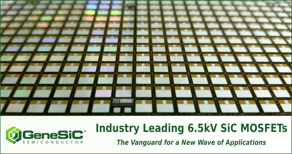
GeneSiC Semiconductor, a pioneer and global supplier of a broad range of Silicon Carbide (SiC) power semiconductors, today announces the immediate availability of 6.5kV SiC MOSFET bare chips – G2R300MT65-CAL and G2R325MS65-CAL. Full SiC modules utilizing this technology are soon to be released. Applications are expected to include traction, pulsed power, smart grid infrastructure and other medium-voltage power converters.

G2R300MT65-CAL – 6.5kV 300mΩ G2R™ SiC MOSFET Bare Chip

G2R325MS65-CAL – 6.5kV 325mΩ G2R™ SiC MOSFET (with Integrated-Schottky) Bare Chip

G2R100MT65-CAL – 6.5kV 100mΩ G2R™ SiC MOSFET Bare Chip

GeneSiC’s innovation features a SiC double-implanted metal oxide semiconductor (DMOSFET) device structure with a junction barrier schottky (JBS) rectifier integrated into the SiC DMOSFET unit cell. This leading-edge power device can be used in a variety of power conversion circuits in the next generation of power conversion systems. Other significant advantages include more efficient bi-directional performance, temperature independent switching, low switching and conduction losses, reduced cooling requirements, superior long-term reliability, ease of paralleling devices and cost benefits. GeneSiC’s technology offers superior performance and also has the potential to reduce the net SiC material footprint in power converters.

“GeneSiC’s 6.5kV SiC MOSFETs are designed and fabricated on 6-inch wafers to realize low on-state resistance, highest quality, and superior price-performance index. This next-generation MOSFETs technology promises exemplar performance, superior ruggedness and long-term reliability in medium-voltage power conversion applications.” said Dr. Siddarth Sundaresan, VP of Technology at GeneSiC Semiconductor.

GeneSiC’s 6.5kV G2R™ SiC MOSFET technology features –

  • High avalanche (UIS) and short circuit ruggedness
  • Superior QG x RDS(ON) figure of merit
  • Temperature independent switching losses
  • Low capacitances and low gate charge
  • Low losses at all temperatures
  • Normally-off stable operation up to 175°C
  • +20 V / -5 V gate drive

For datasheet and other resources, visit – www.genesicsemi.com/sic-mosfet/bare-chip or contact sales@genesicsemi.com

About GeneSiC Semiconductor, Inc.

GeneSiC Semiconductor is a pioneer and world leader in Silicon Carbide technology, while also invested in high power Silicon technologies. The global leading manufacturers of industrial and defense systems depend on GeneSiC’s technology to elevate the performance and efficiency of their products. GeneSiC’s electronic components run cooler, faster, and more economically, and play a key role in conserving energy in a wide array of high power systems. We hold leading patents on wide band gap power device technologies; a market that is projected to reach more than $1 billion by 2022. Our core competency is to add more value to our customers’ end product. Our performance and cost metrics are setting standards in the Silicon Carbide industry.

GeneSiC wins the prestigious R&D100 Award for SiC-Based Monolithic Transistor-Rectifier Switch

DULLES, VA, December 5, 2019 — R&D Magazine has selected GeneSiC Semiconductor Inc. of Dulles, VA as a recipient of the prestigious 2019 R&D 100 Award for development of SiC-Based Monolithic Transistor-Rectifier Switch.

GeneSiC Semiconductor Inc, a key innovator in the Silicon Carbide based power devices was honored with the announcement that it has been awarded the prestigious 2019 R&D 100 Award. This award recognizes GeneSiC for introducing one of the most significant, newly introduced research and development advances among multiple disciplines during 2018. R&D Magazine recognized GeneSiC’s medium voltage SiC power device technology for its ability to monolithically integrate MOSFET and Schottky rectifier on a single chip. These capabilities achieved by GeneSiC’s device critically enable power electronics researchers to develop next-generation power electronic systems like inverters and DC-DC converters. This will allow product developments within electric vehicles, charging infrastructure, renewable energy and energy storage industries. GeneSiC has booked orders from multiple customers towards demonstration of advanced power electronics hardware using these devices and continues to develop its family of Silicon Carbide MOSFET products. The R&D on early version for power conversion applications were developed through US Dept. of Energy and collaboration with Sandia National Laboratories.

The annual technology competition run by R&D Magazine evaluated entries from various companies and industry players, research organizations and universities around the world. The magazine’s editors and a panel of outside experts served as judges, evaluating each entry in terms of its importance to the world of science and research.

According to R&D Magazine, winning an R&D 100 Award provides a mark of excellence known to industry, government, and academia as proof that the product is one of the most innovative ideas of the year. This award recognizes GeneSiC as a global leader in the creation of technology-based products that make a difference in how we work and live.

About GeneSiC Semiconductor, Inc.

GeneSiC is a fast emerging innovator in the area of SiC power devices and has a strong commitment to the development of Silicon Carbide (SiC) based devices for: (a) HV-HF SiC devices for Power Grid, Pulsed power and Directed Energy Weapons; and (b) High temperature SiC power devices for aircraft actuators and oil exploration. GeneSiC Semiconductor Inc. develops Silicon Carbide (SiC) based semiconductor devices for high temperature, radiation, and power grid applications. This includes development of rectifiers, FETs, bipolar devices as well as particle & photonic detectors. GeneSiC has access to an extensive suite of semiconductor design, fabrication, characterization and testing facilities for such devices. GeneSiC capitalizes on its core competency in device and process design to develop the best possible SiC devices for its customers. The company distinguishes itself by providing high quality products that are specifically tuned to each customer’s requirements. GeneSiC has prime/sub-contracts from major US Government agencies including ARPA-E, US Dept of Energy, Navy, DARPA, Dept of Homeland Security, Dept of Commerce and other departments within the US Dept. of Defense. GeneSiC continues to rapidly enhance the equipment and personnel infrastructure at its Dulles, Virginia facility. The company is aggressively hiring personnel experienced in compound semiconductor device fabrication, semiconductor testing and detector designs. Additional information about the company and its products may be obtained by calling GeneSiC at 703-996-8200 or by visiting www.genesicsemi.com.