G3R™ 750V SiC MOSFETs Offer Unparalleled Performance and Reliability

750V G3R SiC MOSFET

DULLES, VA, June 04, 2021 — GeneSiC’s next-generation 750V G3R™SiC MOSFETs will deliver unprecedented levels of performance, robustness and quality that exceeds its counterparts. System benefits include low on-state drops at operating temperatures, faster switching speeds, increased power density, minimal ringing (low EMI) and compact system size. GeneSiC’s G3R™, offered in optimized low-inductance discrete packages (SMD and through hole), are optimized to operate with lowest power losses under all operating conditions and ultra-fast switching speeds. These devices have substantially better performance levels as compared to contemporary SiC MOSFETs.
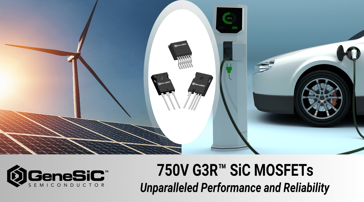
750V G3R SiC MOSFET

“High-efficiency energy usage has become a critical deliverable in next-generation power converters and SiC power devices continue to be the key components driving this revolution. After years of development work towards achieving the lowest on-state resistance and robust short circuit and avalanche performance, we are excited to release the industry’s best performing 750V SiC MOSFETs. Our G3R™ enable power electronics designers to meet the challenging efficiency, power density and quality goals in applications like solar inverters, EV on-board chargers and server/telecom power supplies. An assured quality, supported by fast turn-around and automotive-qualified high volume manufacturing further enhances their value proposition. ” said Dr. Ranbir Singh, President at GeneSiC Semiconductor.

Features –

  • Industry’s lowest gate charge (QG) and internal gate resistance (RG(INT))
  • Lowest RDS(ON) change with temperature
  • Low output capacitance (COSS) and miler capacitance (CGD)
  • 100% avalanche (UIL) tested during production
  • Industry-leading short circuit withstand capability
  • Fast and reliable body diode with low VF and low QRR
  • High and stable gate threshold voltage (VTH) across all temperature and drain-bias conditions
  • Advanced packaging technology for lower thermal resistance and lower ringing
  • Manufacturing uniformity of RDS(ON), VTH and breakdown voltage (BV)
  • Comprehensive product portfolio and safer supply chain with automotive-qualified high volume manufacturing

Applications –

  • Solar (PV) Inverters
  • EV / HEV Onboard Chargers
  • Server & Telecom Power Supplies
  • Uninterruptible Power Supplies (UPS)
  • DC-DC Converters
  • Switched Mode Power Supplies (SMPS)
  • Energy Storage and Battery Charging
  • Induction Heating

All of GeneSiC Semiconductor’s SiC MOSFETs are targeted for automotive applications (AEC-Q101) and PPAP-capable.

G3R60MT07J – 750V 60mΩ TO-263-7 G3R&trade SiC MOSFET

G3R60MT07K – 750V 60mΩ TO-247-4 G3R&trade SiC MOSFET

G3R60MT07D – 750V 60mΩ TO-247-3 G3R&trade SiC MOSFET

For datasheet and other resources, visit – www.genesicsemi.com/sic-mosfet/ or contact sales@genesicsemi.com

All devices are available for purchase through authorized distributors – www.genesicsemi.com/sales-support

Digi-Key Electronics

Newark Farnell element14

Mouser Electronics

Arrow Electronics

About GeneSiC Semiconductor, Inc.

GeneSiC Semiconductor is a pioneer and world leader in Silicon Carbide technology, while also invested in high power Silicon technologies. The global leading manufacturers of industrial and defense systems depend on GeneSiC’s technology to elevate the performance and efficiency of their products. GeneSiC’s electronic components run cooler, faster, and more economically, and play a key role in conserving energy in a wide array of high power systems. We hold leading patents on wide band gap power device technologies; a market that is projected to reach more than $1 billion by 2022. Our core competency is to add more value to our customers’ end product. Our performance and cost metrics are setting standards in the Silicon Carbide industry.

GeneSiC wins the prestigious R&D100 Award for SiC-Based Monolithic Transistor-Rectifier Switch

DULLES, VA, December 5, 2019 — R&D Magazine has selected GeneSiC Semiconductor Inc. of Dulles, VA as a recipient of the prestigious 2019 R&D 100 Award for development of SiC-Based Monolithic Transistor-Rectifier Switch.

GeneSiC Semiconductor Inc, a key innovator in the Silicon Carbide based power devices was honored with the announcement that it has been awarded the prestigious 2019 R&D 100 Award. This award recognizes GeneSiC for introducing one of the most significant, newly introduced research and development advances among multiple disciplines during 2018. R&D Magazine recognized GeneSiC’s medium voltage SiC power device technology for its ability to monolithically integrate MOSFET and Schottky rectifier on a single chip. These capabilities achieved by GeneSiC’s device critically enable power electronics researchers to develop next-generation power electronic systems like inverters and DC-DC converters. This will allow product developments within electric vehicles, charging infrastructure, renewable energy and energy storage industries. GeneSiC has booked orders from multiple customers towards demonstration of advanced power electronics hardware using these devices and continues to develop its family of Silicon Carbide MOSFET products. The R&D on early version for power conversion applications were developed through US Dept. of Energy and collaboration with Sandia National Laboratories.

The annual technology competition run by R&D Magazine evaluated entries from various companies and industry players, research organizations and universities around the world. The magazine’s editors and a panel of outside experts served as judges, evaluating each entry in terms of its importance to the world of science and research.

According to R&D Magazine, winning an R&D 100 Award provides a mark of excellence known to industry, government, and academia as proof that the product is one of the most innovative ideas of the year. This award recognizes GeneSiC as a global leader in the creation of technology-based products that make a difference in how we work and live.

About GeneSiC Semiconductor, Inc.

GeneSiC is a fast emerging innovator in the area of SiC power devices and has a strong commitment to the development of Silicon Carbide (SiC) based devices for: (a) HV-HF SiC devices for Power Grid, Pulsed power and Directed Energy Weapons; and (b) High temperature SiC power devices for aircraft actuators and oil exploration. GeneSiC Semiconductor Inc. develops Silicon Carbide (SiC) based semiconductor devices for high temperature, radiation, and power grid applications. This includes development of rectifiers, FETs, bipolar devices as well as particle & photonic detectors. GeneSiC has access to an extensive suite of semiconductor design, fabrication, characterization and testing facilities for such devices. GeneSiC capitalizes on its core competency in device and process design to develop the best possible SiC devices for its customers. The company distinguishes itself by providing high quality products that are specifically tuned to each customer’s requirements. GeneSiC has prime/sub-contracts from major US Government agencies including ARPA-E, US Dept of Energy, Navy, DARPA, Dept of Homeland Security, Dept of Commerce and other departments within the US Dept. of Defense. GeneSiC continues to rapidly enhance the equipment and personnel infrastructure at its Dulles, Virginia facility. The company is aggressively hiring personnel experienced in compound semiconductor device fabrication, semiconductor testing and detector designs. Additional information about the company and its products may be obtained by calling GeneSiC at 703-996-8200 or by visiting www.genesicsemi.com.

GeneSiC wins $2.53M from ARPA-E towards development of Silicon Carbide Thyristor-based devices

DULLES, VA, September 28, 2010 – Advanced Research Projects Agency – Energy (ARPA-E) has entered into a Cooperative Agreement with the GeneSiC Semiconductor-led team towards the development of the novel ultra high-voltage silicon carbide (SiC) Thyristor based devices. These devices are expected to be key enablers for integrating large-scale wind and solar power plants into the next-generation Smart Grid.

“This highly competitive award to GeneSiC will allow us to extend our technical leadership position in the multi-kV Silicon Carbide technology, as well as our commitment to grid-scale alternative energy solutions with solid state solutions,” commented Dr. Ranbir Singh, President of GeneSiC. “Multi-kV SiC Thyristors we’re developing are the key enabling technology towards the realization of Flexible AC Transmission Systems (FACTS) elements and High Voltage DC (HVDC) architectures envisaged towards an integrated, efficient, Smart Grid of the future. GeneSiC’s SiC-based Thyristors offer 10X higher voltage, 100X faster switching frequencies and higher temperature operation in FACTS and HVDC power processing solutions as compared to conventional Silicon-based Thyristors.”

In April 2010, GeneSiC responded to the Agile Delivery of Electrical Power Technology (ADEPT) solicitation from ARPA-E that sought to invest in materials for fundamental advances in high voltage switches that has the potential to leapfrog existing power converter performance while offering reductions in cost. The company’s proposal titled “Silicon Carbide Anode Switched Thyristor for medium voltage power conversion” was selected to provide a lightweight, solid-state, medium voltage energy conversion for high power applications such as solid-state electrical substations and wind turbine generators. Deploying these advanced power semiconductor technologies could provide as much as a 25-30 percent reduction in electricity consumption through increased efficiencies in delivery of electrical power. Innovations selected were to support and promote U.S. businesses through technological leadership, through a highly competitive process.

Silicon carbide is a next-generation semiconductor material with vastly superior properties to conventional silicon, such as the ability to handle ten times the voltage—and one-hundred times the current—at temperatures as high as 300ºC. These characteristics make it ideally suited to high-power applications such as hybrid and electric vehicles, renewable energy (wind and solar) installations, and electrical-grid control systems.

It is now well established that ultra-high voltage (>10kV) Silicon Carbide (SiC) device technology will play a revolutionary role in the next-generation utility grid. Thyristor-based SiC devices offer the highest on-state performance for >5 kV devices, and are widely applicable towards medium voltage power conversion circuits like Fault-Current Limiters, AC-DC converters, Static VAR Compensators and Series Compensators. SiC based Thyristors also offer the best chance of early adoption due to their similarities to conventional power grid elements. Other promising applications and advantages for these devices include:

  • Power-management and power-conditioning systems for Medium Voltage DC conversion sought under Future Naval Capability (FNC) of US Navy, Electro-magnetic launch systems, high energy weapon systems and medical imaging. The 10-100X higher operating frequency capability allows unprecedented improvements in size, weight, volume and ultimately, cost of such systems.
  • A variety of energy storage, high-temperature and high-energy physics applications. Energy storage and power grid applications are receiving increasing attention as the world focuses on more efficient and cost-effective energy-management solutions.

GeneSiC is a fast emerging innovator in the area of SiC power devices and has a strong commitment to the development of Silicon Carbide (SiC) based devices for: (a) HV-HF SiC devices for Power Grid, Pulsed power and Directed Energy Weapons; and (b) High temperature SiC power devices for aircraft actuators and oil exploration.

“We’ve emerged as a leader in ultra-high voltage SiC technology by leveraging our core competency in device and process design with an extensive suite of fabrication, characterization, and test facilities,” concludes Dr. Singh. “GeneSiC’s position has now been effectively validated by the US DOE with this significant follow-on award.”

About GeneSiC Semiconductor

Strategically located near Washington, DC in Dulles, Virginia, GeneSiC Semiconductor Inc. is a leading innovator in high-temperature, high-power and ultra high-voltage silicon carbide (SiC) devices. Current development projects include high-temperature rectifiers, SuperJunction Transistors (SJT) and a wide variety of Thyristor based devices. GeneSiC has or has had prime/sub-contracts from major US Government agencies, including the Department of Energy, Navy, Army, DARPA, and the Department of Homeland Security. The company is currently experiencing substantial growth, and hiring qualified personnel in power-device and detector design, fabrication, and testing. To find out more, please visit www.genesicsemi.com.