DULLES, VA, February 12, 2020 — GeneSiC Semiconductor’s next-generation 1200V G3R™SiC MOSFETs with RDS(ON) levels ranging from 20 mΩ to 350 mΩ deliver unprecedented levels of performance, robustness and quality that exceeds its counterparts. System benefits include higher efficiency, faster switching frequency, increased power density, reduced ringing (EMI) and compact system size.
GeneSiC announces the availability of its industry-leading 3rd generation Silicon Carbide MOSFETs that feature industry-leading performance, robustness and quality to harness never before seen levels of efficiency and system reliability in automotive and industrial applications.
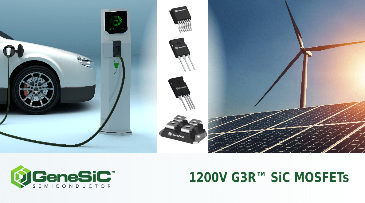
These G3R™ SiC MOSFETs, offered in optimized low-inductance discrete packages (SMD and through hole), are highly optimized for power system designs requiring elevated efficiency levels and ultra-fast switching speeds. These devices have substantially better performance levels as compared to competing products. An assured quality, supported by fast turn-around high volume manufacturing further enhances their value proposition.
“After years of development work towards achieving the lowest on-state resistance and enhanced short circuit performance, we are excited to release the industry’s best performing 1200V SiC MOSFETs with over 15+ discrete and bare chip products. If the next-generation power electronics systems are to meet the challenging efficiency, power density and quality goals in applications like automotive, industrial, renewable energy, transportation, IT and telecom, then they require significantly improved device performance and reliability as compared to presently available SiC MOSFETs” said Dr. Ranbir Singh, President at GeneSiC Semiconductor.
Features –
- Superior QG x RDS(ON) figure-of-merit – G3R™ SiC MOSFETs feature the industry’s lowest on-state resistance with a very low gate charge, resulting in to 20% better figure-of-merit than any other similar competitor device
- Low conduction losses at all temperatures – GeneSiC’s MOSFETs feature the softest temperature dependence of on-state resistance to offer very low conduction losses at all temperatures; significantly better than any other trench and planar SiC MOSFETs in the market
- 100 % avalanche tested – Robust UIL capability is a critical requirement for the majority of field applications. GeneSiC’s 1200V SiC MOSFET discrete are 100 % avalanche (UIL) tested during production
- Low gate charge and low internal gate resistance – These parameters are critical towards realizing ultra-fast switching and achieving highest efficiencies (low Eon -Eoff) across a wide range of application switching frequencies
- Normally-off stable operation up to 175°C – All of GeneSiC’s SiC MOSFETs are designed and fabricated with state-of-the-art processes to deliver products that are stable and reliable at all operating conditions without any malfunction risk. The superior gate oxide quality of these devices prevents any threshold (VTH) drift
- Low device capacitances – G3R™ are designed to drive faster and more efficient with their low device capacitances – Ciss, Coss and Crss
- Fast and reliable body diode with low intrinsic charge – GeneSiC’s MOSFETs feature benchmark low reverse recovery charge (QRR) at all temperatures; 30% better than any similarly rated competitor device. This offers further reduction in power losses and boosts operating frequencies
- Ease of use – G3R™ SiC MOSFETs are designed to be driven at +15V / -5V gate drive. This offers broadest compatibility with existing commercial IGBT and SiC MOSFET gate drivers
Applications –
- Electric Vehicle – Power Train and Charging
- Solar Inverter and Energy Storage
- Industrial Motor Drive
- Uninterruptible Power Supply (UPS)
- Switched Mode Power Supply (SMPS)
- Bi-directional DC-DC converters
- Smart Grid and HVDC
- Induction Heating and Welding
- Pulsed Power Application
All devices are available for purchase through authorized distributors – www.genesicsemi.com/sales-support
For datasheet and other resources, visit – www.genesicsemi.com/sic-mosfet or contact sales@genesicsemi.com
All of GeneSiC Semiconductor’s SiC MOSFETs are targeted for automotive applications (AEC-Q101) and PPAP-capable. All devices are offered in industry standard D2PAK, TO-247 and SOT-227 packages.
About GeneSiC Semiconductor, Inc.
GeneSiC Semiconductor is a pioneer and world leader in Silicon Carbide technology, while also invested in high power Silicon technologies. The global leading manufacturers of industrial and defense systems depend on GeneSiC’s technology to elevate the performance and efficiency of their products. GeneSiC’s electronic components run cooler, faster, and more economically, and play a key role in conserving energy in a wide array of high power systems. We hold leading patents on wide band gap power device technologies; a market that is projected to reach more than $1 billion by 2022. Our core competency is to add more value to our customers’ end product. Our performance and cost metrics are setting standards in the Silicon Carbide industry.